Delivery method of calculation
Pubtime:2018/01/04
All orders delivery method of calculation:
All delivery on weekdays (Sunday, national holidays) is not included
Order after 16:00 the same day, delivery from the next day began to calculate.
More> >>
Confidentiality agreement template
Pubtime:2018/01/04
Confidentiality agreement
The company is located in:
Party A: Shenzhen Kai new Albert CHAN Electronics Co., Ltd.
Party B:
Both parties to the contract should follow the following principles:
1. Information to be kept confidential
1.1 All the parties mentioned in this Co...
More> >>

Pricing considerations
Pubtime:2018/01/04
Sales tax
1, an increase of 6% (VAT, low deduction 3%)
The sales price is the sum of 'Subtotal' plus 'Sales Tax'
2, 17% value added (VAT, can deduct 17%)
The sales price is the sum of 'Subtotal' plus 'Sales Tax'
Shipping costs
When the total price of goods...
More> >>
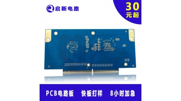
Order common problems
Pubtime:2018/01/10
System board and offer information to be provided
1 GERBER or PCB file
2 materials, quantity requirements and surface treatment, other special requirements
3 development must provide the development of functional specifications
4 copy board to provide two sets of original copy board
5 decryption I...
More> >>
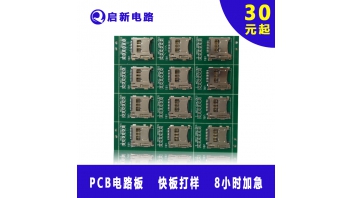
System board common problems
Pubtime:2018/01/04
Surface treatment of the minimum molding size
Silver, tin, Entek molding the following minimum size:
Silver 90 * 55mm
Tin 100 * 150mm
Entek 90 * 55mm
Surface treatment such as one of the above, the single-chip size, smaller than the corresponding size, we will typeset ship...
More> >>
PCB版设计主要步骤是什么?
Pubtime:2018/02/24
First, the circuit board design work PCB design system
1, the use of schematic design tools to draw schematics, and generate the corresponding network table. Of course, in some special cases, such as the circuit board is relatively simple, there is already a network table and other cases can not be ...
More> >>