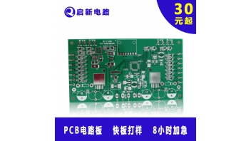
PCB design in the production of the problem and solution
Pubtime:2018/02/24
Substrate in the PCB design process may have the following problems
one. Solder a variety of issues
Signs of the phenomenon: cold solder joints or solder bursting holes.
Inspection methods: Pre-dipped and dip-welded after holes on the regular analysis, in order to find the place where the ...
More> >>
Electroless nickel / gold production management experience learning
Pubtime:2018/02/24
Electroless nickel / gold production management is currently responsible for one of the wet treatment production lines. The line is a manual production line, no traffic lifting, thanks to manual mention, discharge nickel / gold plate production. In addition, in recent years, as surface coating incre...
More> >>